
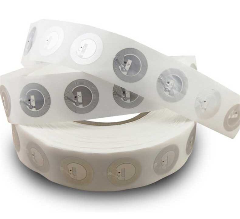
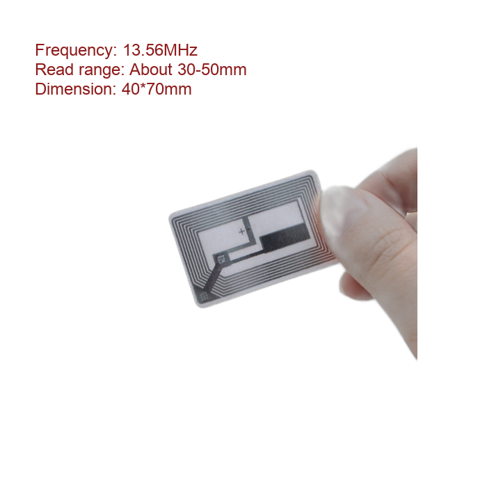
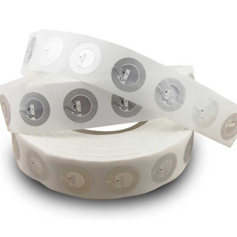
An NFC tag inlay is the core component of an NFC (Near Field Communication) tag, consisting of a microchip and an antenna mounted on a thin, flexible substrate. It serves as the digital identity that can store information and communicate wirelessly with NFC-enabled devices like smartphones. Typical specifications include chip type (NTAG213, NTAG216, etc.), memory (144–888 bytes), operating frequency (13.56 MHz), size (various, e.g., 25×25 mm, 50×50 mm), and read/write distance (up to 10 cm). NFC tag inlays are used for product authentication, contactless payments, smart packaging, access control, and marketing campaigns, addressing challenges like counterfeiting, manual data entry, and inefficient customer engagement.
- Date
- July 11, 2026
The NTAG424 DNA Inlay is a high-security NFC inlay designed specifically for label manufacturers who require reliable anti-counterfeiting and data protection at a competitive price point. It features:
- Advanced Security: NXP NTAG424 DNA chip with AES-128 encryption, SUN, and SDM for secure data transmission and tamper detection.
- Universal Compatibility: NFC Forum Type 4 compliant and ISO/IEC 14443A certified, ensuring seamless read/write with all modern smartphones and NFC readers.
- Cost‑Effective for Converters: Optimized manufacturing process delivers the lowest cost in its class, making large-volume label production profitable without compromising security.
- Date
- June 18, 2026
The 40 * 70mm custom 13.56MHz RFID embedded self-adhesive label NFC PVC coated paper label ICODE SLIX2 chip is a high-performance NFC paper label designed for industrial asset tracking and secure data management. Produced by DO RFID Reader manufacturer, it provides reliable performance for professional industrial systems. It features:
- Unique Identifier (UID): A factory-locked UII ensures each tag has a unique identity, preventing data conflicts in large-scale inventory systems.
- Password-Protected Memory: Each page is secured by a 32-bit password, protecting sensitive user data from unauthorized read/write access for industrial asset tracking and anti-counterfeiting.
- Privacy Mode Function: A 32-bit privacy password enables the tag to hide its presence, meeting strict data protection requirements for secure NFC deployments.


Description
They are easily hidden behind a poster or display, or inside a product housing or package; or they may be imprinted with high-visibility graphics, attracting the attention of people with smartphones or other standard RFID readers.
Promotional marketers use the NFC tag inlay to quickly and cost-effectively integrate digital touch points into physical media, such as posters, packaging, point-of-purchase displays, and magazines.
With Inlays & Labels in place, smartphone-wielding customers can interact in real time with your brand. Wireless technology enables effortless transactions, engaging improved customer participation and satisfaction.
Primary Applications:
- Access control
- Attendance control
- Identification
- Tickets
- E-tickets
Specification
| Material | Base material | Papers / PET / PVC / plastic; 3M glue |
|---|---|---|
| Antenna material | Aluminum etched antenna ; COB + Copper coil | |
| Chip material | original chips | |
| Protocol | ISO 14443A ISO15693 and ISO 18000-6C | |
| Frequency | 13.56MHz (HF) and 860-960MHz (UHF) | |
| Chips | All chips available by request | |
| Reading distance | 0.1~10m(depend on reader, tag and working environment ) | |
| Working mode | read-only or read-write according to chip type | |
| Read/write endurance | >100,000 times | |
| Customized serivice | 1. custom printing logo, text | |
| 2. pre-code: URL, text , numbers | ||
| 3. size, shape | ||
| Packing | 5000pcs/roll ,1-4roll/carton,or by customized | |
| Working temperature | -25℃ to+85℃ | |
| Applied field | logistics management, apparel management, library book management, wines management and the application of bags, trays and luggage,etc | |
An NFC tag inlay is the electronic core of an NFC sticker, smart label, card, or embedded identification product. It combines a microchip and antenna on a thin substrate, allowing compatible smartphones and NFC readers to exchange information through short-range wireless communication.
For label manufacturers, RFID converters, packaging companies, and brand protection providers, sourcing the right NFC tag inlay is an important step in developing reliable smart labels. The chip determines available memory and security functions, while the antenna design, substrate, and production format influence reading performance and compatibility with downstream converting equipment.
However, selecting an NFC inlay involves more than choosing an NTAG213 or NTAG216 chip. Buyers also need to consider dry and wet inlay formats, antenna dimensions, die-cut size, roll specifications, adhesive construction, and the requirements of the finished product.
At D.O RFID Group, we manufacture and supply customized RFID and NFC products for industrial, commercial, and consumer applications. Our NFC inlay solutions include standard NFC chips, transparent inlays, specialty antenna configurations, and secure NTAG424 DNA inlays.
This guide explains how NFC inlays work, compares common chip options, examines competing manufacturers’ product approaches, and provides practical advice for B2B buyers planning customized or bulk NFC inlay orders.
What Is an NFC Tag Inlay?
An NFC tag inlay is a semi-finished electronic component consisting primarily of an NFC chip and an antenna mounted on a thin substrate.
It is normally integrated into another product during subsequent manufacturing processes. Depending on its construction, an inlay can become:
- An adhesive NFC sticker
- A printed NFC product label
- An NFC hang tag
- An NFC smart card
- An embedded NFC component
- A smart packaging label
- An NFC wristband or promotional product
The inlay stores an electronic identity and can exchange data with compatible NFC-enabled devices. The user typically interacts with the finished product by bringing a smartphone or NFC reader close to the tag.
A standard NFC inlay contains four main components:
| Component | Material or Structure | Function |
|---|---|---|
| NFC chip | Integrated circuit (IC) | Stores data and manages wireless communication |
| Antenna | Etched aluminum, copper, or another suitable conductor | Creates the electromagnetic coupling required for communication |
| Substrate | PET or another suitable flexible material | Supports the chip and antenna |
| Adhesive layer (optional) | Pressure-sensitive adhesive | Allows the inlay to be attached to a label or packaging surface |
Some inlays are supplied with an adhesive layer and release liner, while others are delivered as dry electronic components for further processing.
According to the NFC Forum, NFC operates through standardized contactless communication technologies, with specifications covering tag communication, data exchange, and interoperability. Source: NFC Forum – Technical Specifications.
For B2B buyers, the most important distinction is that an NFC inlay is not necessarily a finished NFC sticker. It may require additional printing, lamination, adhesive coating, die-cutting, or packaging before it can be applied to the final product.
How Does an NFC Inlay Work?
NFC (Near Field Communication) is a short-range wireless technology based on high-frequency RFID communication.
A standard NFC inlay operates at 13.56 MHz. It normally uses passive technology, meaning the tag does not need an internal battery for ordinary data communication.
The process works as follows:
Step 1: An NFC-enabled device generates a magnetic field.
A smartphone or NFC reader produces a 13.56 MHz electromagnetic field.
Step 2: The inlay antenna receives energy.
The antenna inside the NFC inlay couples with the reader’s field and provides energy to the chip.
Step 3: The chip processes the communication.
The integrated circuit responds according to its supported protocol and retrieves the relevant stored information.
Step 4: Data is transferred to the reader.
The NFC device reads the tag information, which may include a URL, identification number, NDEF message, or application-specific data.
Step 5: The connected application processes the information.
The smartphone or reader can open a website, display product information, connect to a digital service, or perform another programmed function.
For example, a cosmetics manufacturer can embed an NFC inlay into product packaging. When a customer taps the finished label with a compatible smartphone, the phone can open a product information or authentication page.
The inlay provides the electronic connection between the physical package and the digital service.
Dry NFC Inlay vs. Wet NFC Inlay: What Is the Difference?
One of the first decisions for NFC label converters is whether to purchase dry inlays or wet inlays.
The main difference is the adhesive construction.
Dry NFC Inlays
A dry inlay consists of the NFC chip and antenna mounted on a substrate without a pressure-sensitive adhesive and release liner.
It is generally intended for manufacturers that will carry out additional converting processes themselves.
Main characteristics:
- Chip and antenna assembled on a substrate
- No standard pressure-sensitive adhesive backing
- Suitable for customized lamination and embedding
- Can be integrated into cards, packaging, labels, and other products
- Requires downstream processing according to the finished-product design
Best-fit buyers: RFID converters, smart card manufacturers, packaging manufacturers, and businesses with their own lamination or label-converting facilities.
Wet NFC Inlays
A wet inlay includes an adhesive layer and release liner, making it easier to attach to another material during subsequent processing.
Depending on the supplier, the wet inlay may already be die-cut and supplied in reel format.
Main characteristics:
- NFC chip and antenna
- Pressure-sensitive adhesive
- Release liner
- Convenient integration into self-adhesive labels
- Available in suitable roll or sheet formats
Best-fit buyers: Label manufacturers, smart sticker producers, packaging companies, and converters that need adhesive-backed NFC components.
Dry Inlay vs. Wet Inlay vs. Finished NFC Label
| Feature | Dry NFC Inlay | Wet NFC Inlay | Finished NFC Label |
|---|---|---|---|
| NFC chip | Yes | Yes | Yes |
| Antenna | Yes | Yes | Yes |
| Substrate | Yes | Yes | Yes |
| Adhesive | No standard PSA layer | Yes | Yes |
| Release liner | No standard liner | Yes | Usually yes for self-adhesive labels |
| Printed face material | Not necessarily | Not necessarily | Can be included |
| Additional converting | Usually required | May be required | Usually ready for application |
| Main buyer | Inlay converters | Label converters | Brand owners and packaging companies |
Terminology can vary between manufacturers, particularly for wet inlays and finished labels. Buyers should request a layer construction drawing to confirm exactly what is included.
For example, an Identiv NTAG424 DNA product datasheet distinguishes dry inlay, wet inlay, and finished label formats. It also provides separate thickness and converting dimensions for each configuration. This is a useful example of why buyers should compare the complete product structure rather than relying on the product name alone. Source: Identiv – NTAG424 DNA Inlay and Label Datasheet.
Common NFC Inlay Chip Options: NTAG213 vs. NTAG215 vs. NTAG216
Chip selection influences memory capacity, available security functions, and the intended application.
The NXP NTAG21x family is widely used in NFC stickers, smart labels, retail packaging, product identification, and smartphone-interactive products.
The three popular models are NTAG213, NTAG215, and NTAG216.
Technical Comparison
| Specification | NTAG213 | NTAG215 | NTAG216 |
|---|---|---|---|
| Operating Frequency | 13.56 MHz | 13.56 MHz | 13.56 MHz |
| NFC Standard | NFC Forum Type 2 | NFC Forum Type 2 | NFC Forum Type 2 |
| ISO Standard | ISO/IEC 14443 Type A | ISO/IEC 14443 Type A | ISO/IEC 14443 Type A |
| User Memory | 144 bytes | 504 bytes | 888 bytes |
| Total EEPROM Capacity | 180 bytes | 540 bytes | 924 bytes |
| Data Transfer Rate | 106 kbit/s | 106 kbit/s | 106 kbit/s |
| Unique Identifier | 7-byte UID | 7-byte UID | 7-byte UID |
| Write Endurance | 100,000 cycles | 100,000 cycles | 100,000 cycles |
| Data Retention | 10 years | 10 years | 10 years |
| Typical Applications | URLs, basic product information | More extensive NDEF data and gaming applications | Larger data records and more complex applications |
The memory capacities above are from NXP’s official NTAG213/215/216 product documentation. The total EEPROM capacity should not be confused with the freely available user memory. Source: NXP – NTAG213/215/216 Datasheet.
Which Chip Should You Choose?
NTAG213 – For Standard NFC Applications
NTAG213 is generally sufficient for applications such as:
- Website URLs
- Digital contact cards
- Product information links
- Smart posters
- Basic marketing campaigns
- Simple product identification
Its 144-byte user memory is suitable for many short NDEF messages.
NTAG215 – For Medium Data Requirements
NTAG215 provides 504 bytes of user memory. It may be appropriate when an application needs more room for stored data, configuration details, or additional NDEF records.
Typical applications include selected gaming products, interactive merchandise, and smart labels.
NTAG216 – For Larger Memory Requirements
NTAG216 provides 888 bytes of user memory, making it the highest-capacity chip in the NTAG21x family.
It can be considered for applications requiring larger data records or multiple stored information elements.
However, more memory does not automatically provide stronger security. If the project requires advanced authentication, encryption, or secure messaging, a dedicated security chip such as NTAG424 DNA may be more suitable.
NTAG424 DNA NFC Inlay for Product Authentication
For premium packaging, brand protection, and product authentication, the chip selection process should consider security functions rather than memory capacity alone.
NXP NTAG424 DNA is a secure NFC IC designed for applications requiring stronger authentication and data protection.
Its key features include:
- AES-128 cryptographic operations
- Secure Unique NFC (SUN) messages
- Secure Dynamic Messaging (SDM)
- ISO/IEC 14443-A compatibility
- NFC Forum Type 4 Tag compliance
- 416 bytes of total memory
- Configurable security and access controls
The 416-byte memory is organized into a 32-byte capability container, a 256-byte NDEF file, and a 128-byte protected data file. These figures describe the chip’s file structure, not 416 bytes of freely available NDEF memory. Source: NXP – NTAG424 DNA.
How Does SUN Authentication Work?
SUN generates a cryptographically protected message when the tag is read.
A compatible verification system can use this dynamic information to verify the tag rather than relying only on a static serial number or URL.
This is useful for:
- Luxury product authentication
- Cosmetics and skincare
- Wine and spirits
- Pharmaceuticals and healthcare products
- Electronics
- Secure supply chain applications
However, installing an NTAG424 DNA chip does not automatically create a complete anti-counterfeiting system.
The brand owner or solution provider still needs to configure cryptographic keys, implement the verification process, and manage the authentication service appropriately.
DO RFID NTAG424 DNA Inlay
DO RFID supplies customized NTAG424 DNA inlays designed for label manufacturers and smart packaging converters.
According to the published product specification, the inlay uses a PET substrate and supports customization of antenna design and UID encoding.
| Parameter | Published Specification |
|---|---|
| Product Type | NFC Inlay |
| Chip | NXP NTAG424 DNA |
| Frequency | 13.56 MHz |
| Memory | 416 bytes total chip memory |
| Protocol | ISO/IEC 14443-A |
| NFC Standard | NFC Forum Type 4 |
| Security | AES-128, SUN, SDM |
| Substrate | PET |
| Available Sizes | Multiple sizes; customized options |
| Operating Temperature | -25°C to +60°C |
| IP Rating | Not applicable to bare inlay |
| Customization | Antenna design, UID encoding |
| Published MOQ | 5,000 pieces |
| Published Lead Time | 15–20 days |
These are published product-page details. Final MOQ and lead time should be reconfirmed when requesting a quotation, particularly for customized antenna designs or pre-encoding. DO RFID – NTAG424 DNA Inlay.
For buyers developing high-security smart packaging, our NTAG424 DNA NFC Inlay can be evaluated as a starting point for customized label development.
NFC Inlay Antenna Design: Why Size and Geometry Matter
The antenna is one of the most important elements of an NFC inlay.
Even when two inlays use the same chip, their reading performance can differ because of antenna size, shape, number of turns, conductor material, tuning, and the surrounding environment.
Common NFC Antenna Materials
| Antenna Type | Main Characteristics | Typical Applications |
|---|---|---|
| Etched aluminum antenna | Thin conductive structure suitable for many high-volume inlays | General NFC stickers and labels |
| Copper antenna | High-conductivity antenna construction | Selected compact or specialty designs |
| Wire-wound copper coil | Wire-based antenna construction | Selected card, tag, and specialty formats |
| Customized antenna | Designed according to chip, dimensions, and application | Space-constrained or specialized NFC products |
The selection should account for manufacturing feasibility as well as electrical performance.
Antenna Dimensions vs. Die-Cut Dimensions
One common sourcing mistake is assuming the antenna size and finished inlay size are identical.
They are separate specifications:
- Antenna dimensions: The physical dimensions of the conductive antenna structure.
- Die-cut dimensions: The finished outline of the adhesive-backed inlay or label.
- Overall inlay dimensions: The dimensions of the complete chip-and-antenna assembly, including any required connecting sections or tails.
For example, Avery Dennison’s Midas NFC inlay uses a 10 × 17 mm antenna with an NXP NTAG213 chip, while its Circus NFC product uses a 20 mm antenna and a 22 mm die-cut size. The separate values illustrate why antenna size and finished product dimensions must be specified independently. Sources: Avery Dennison Midas NFC and Avery Dennison Circus NFC.
What Determines NFC Reading Distance?
NFC operates over short distances. NXP lists an operating distance of up to 100 mm for the NTAG213/215/216 chip family, depending on field strength, antenna geometry, and other parameters. This is a chip-level reference, not a guaranteed reading distance for every finished inlay. Source: NXP NTAG21x Product Specifications.
Actual performance depends on:
- Antenna dimensions and geometry.
- Reader antenna size and alignment.
- Chip sensitivity.
- Antenna resonance and tuning.
- Distance between the reader and tag.
- Product housing and substrate materials.
- Nearby metal or other RF-interfering materials.
NXP’s antenna design guidance emphasizes the importance of matching reader and tag antenna geometry to improve coupling and NFC performance. It also discusses the role of ferrite shielding for selected metal-adjacent applications. Source: NXP – NFC Antenna Design Made Easy.
Our recommendation: Do not choose an NFC inlay only by its nominal antenna size. Test the actual inlay with the intended smartphone or reader, inside the finished product or packaging structure.
Can an NFC Inlay Work on Metal?
A standard NFC inlay is not automatically suitable for direct attachment to metal.
Metal can alter the antenna’s electromagnetic environment, affecting resonance and communication performance. When an NFC label is installed directly on a metal surface, its performance may decrease significantly or fail entirely.
For metal-mounted applications, a dedicated anti-metal NFC construction may be required. This often uses a ferrite layer or another suitable shielding and antenna arrangement.
When developing an anti-metal NFC inlay, consider:
- Metal surface type
- Required label size
- Ferrite material and thickness
- Antenna geometry
- Adhesive construction
- Mounting position
- Actual NFC reader or smartphone performance
DO RFID also provides small micro FPC NTAG213 on-metal NFC tags for compact metal-mounted identification applications.
This is a separate product construction from an ordinary transparent or standard PET NFC inlay. Buyers should specify whether the tag needs to work directly on metal before ordering.
Custom NFC Inlay Specifications for B2B Buyers
NFC inlays are often purchased by label converters and manufacturers that need specific dimensions, reel formats, chip configurations, and electrical characteristics.
A complete specification should cover more than the chip and operating frequency.
Standard Technical Specification Framework
| Parameter | Common Options or Requirements |
|---|---|
| Product Type | Dry inlay, wet inlay, finished NFC label |
| Operating Frequency | 13.56 MHz |
| Chip | NTAG213, NTAG215, NTAG216, NTAG424 DNA, MIFARE Ultralight EV1, or other compatible IC |
| Protocol | ISO/IEC 14443-A, NFC Forum Type 2 or Type 4, according to chip |
| Antenna Material | Aluminum, copper, or suitable specialty construction |
| Base Material | PET, paper, or other specified substrate |
| Antenna Shape | Round, rectangular, square, customized geometry |
| Antenna Dimensions | Customized according to design |
| Finished Inlay Size | Customized |
| Die-Cut Shape | Round, square, rectangular, or irregular |
| Adhesive | None for dry inlay; selected PSA for wet inlay |
| Release Liner | Paper or film, depending on construction |
| Encoding | UID-related processing, NDEF data, URL, or customer-defined data where supported |
| Supply Format | Reel, sheet, or individual pieces |
| Roll Pitch | Customized according to converting equipment |
| Web Width | Confirmed according to production-line requirements |
| Core Diameter | Customized or selected from standard options |
| Application | Smart labels, product authentication, packaging, access control, tickets, and marketing |
The exact options depend on the chip, antenna design, substrate, converting format, and order requirements.
Reel Specifications: What NFC Label Converters Should Not Overlook
For label manufacturers, the electrical performance of an NFC inlay is only one part of the purchasing decision.
The reel must also fit the downstream converting equipment.
Important details include:
| Reel Parameter | Why It Matters |
|---|---|
| Web width | Must match the production machine’s usable material width |
| Pitch | Determines the spacing between consecutive inlays |
| Core diameter | Must fit the machine’s unwinding shaft |
| Maximum roll diameter | Must remain within machine capacity |
| Winding direction | Determines how the inlay enters the converting or dispensing process |
| Quantity per reel | Affects production planning and material handling |
| Splice limit | Influences production continuity |
| Marking of defective units | Helps downstream inspection and rejection |
| Inlay position | Ensures accurate alignment with printing or die-cutting operations |
For example, Identiv’s NTAG424 DNA datasheet provides an antenna size, overall tag dimensions, pitch, web width, and thickness separately. This shows why converter-oriented specifications are more useful than a simple statement such as “NTAG424 inlay, 13.56 MHz.” Source: Identiv NTAG424 DNA Technical Datasheet.
When requesting samples, label converters should provide their machinery specifications whenever possible. This allows the supplier to assess whether the selected inlay construction can be processed efficiently.
NFC Inlay Applications Across Different Industries
1. Smart Product Packaging
NFC inlays can be embedded into product packaging to connect physical products with digital information.
A smartphone tap may open:
- Product instructions
- Brand websites
- Product registration pages
- Promotional content
- Warranty information
- Product verification services
For packaging manufacturers, the inlay should be thin enough and dimensionally suitable for integration into the selected carton, label, or packaging structure.
2. Anti-Counterfeiting and Product Authentication
Secure NFC chips such as NTAG424 DNA can support product authentication by generating cryptographically protected dynamic messages.
They are particularly relevant to:
- Luxury goods
- Cosmetics
- Wine and spirits
- Electronics
- Pharmaceuticals
- Premium branded merchandise
However, a chip alone does not provide a complete anti-counterfeiting solution. Cryptographic keys, message validation, backend infrastructure, and brand-side security procedures must also be implemented.
3. Apparel and Fashion
NFC inlays can be incorporated into clothing labels, hang tags, footwear labels, and other product identification components.
Potential functions include product information, digital engagement, and authentication.
Avery Dennison’s Midas NFC product, for example, uses a compact 10 × 17 mm antenna with an NTAG213 chip and is designed for space-constrained products. Its published applications include apparel, electronics, and gaming. Source: Avery Dennison Midas NFC.
4. Retail Marketing and Smart Advertising
NFC inlays can be embedded into posters, promotional displays, magazines, product shelves, and point-of-purchase materials.
Customers can interact with the physical object using an NFC-enabled smartphone.
This reduces the need for manual URL entry and provides a simple connection between printed media and digital content.
5. Access Control and Ticketing
Depending on the selected chip, protocol, and system architecture, NFC inlays can be incorporated into access cards, tickets, passes, and other contactless identification products.
The chip should be selected according to the reader infrastructure and security requirements rather than assuming that all NFC chips can replace one another.
NFC Inlay Supplier Comparison: What Do Competing Manufacturers Offer?
A review of product pages and technical datasheets from NFC inlay suppliers shows several distinct approaches to product development.
Some focus on compact antenna designs, while others emphasize secure chips, reel formats, or high-volume inlay manufacturing.
| Manufacturer / Brand | Published NFC Inlay Product | Main Technical Focus | B2B Purchasing Consideration |
|---|---|---|---|
| Avery Dennison | Midas NFC, Midas+ NFC, Circus NFC | Compact antenna sizes, NTAG chips, different inlay formats | Small-footprint applications and established inlay product families |
| OSRFID | OS-Φ27-NTAG | 27 mm antenna, NTAG213/215/216, dry/wet/label formats | Multiple delivery formats and chip options |
| Identiv | ID-A514 NTAG424 DNA | 416-byte chip, dry/wet/label versions, detailed reel specifications | Converter-ready technical documentation |
| ID RFID | NTAG213/215/216 NFC inlays | Dry and wet inlays, custom antenna design, reel supply | Customized antenna and bulk converter supply |
| DO RFID | NTAG424 DNA, transparent NTAG213, MIFARE Ultralight EV1 | Multiple chip and substrate options, custom antenna and product integration | Customized NFC inlays and related finished NFC products |
These comparisons are based on published product information, not independent factory audits or comparative performance tests.
Avery Dennison: Compact Antenna Design
Avery Dennison’s Midas NFC family demonstrates how antenna geometry can be optimized for smaller products.
Its published Midas specification includes an NTAG213 chip and a 10 × 17 mm antenna, while Circus NFC uses a 20 mm round antenna with a 22 mm die-cut size. These examples are particularly useful for buyers developing inlays for small packaging, retail items, and embedded product applications. (Avery Dennison Midas NFC; Avery Dennison Circus NFC).
OSRFID: Multiple Inlay Delivery Formats
OSRFID’s OS-Φ27-NTAG product specifies a 27 mm antenna and options for NTAG213, NTAG215, and NTAG216 chips.
It also publishes dry inlay, wet inlay, and label formats, giving converters different ways to integrate the NFC component into their production processes. The company describes using Mühlbauer DDA equipment and Voyantic Tagformance testing in its manufacturing operations. Source: OSRFID – OS-Φ27-NTAG.
Identiv: Detailed Converter Specifications
Identiv’s ID-A514 NTAG424 DNA datasheet provides different specifications for dry inlays, wet inlays, and finished labels.
Its published antenna dimensions are approximately 67 × 25 mm including the tail, with separate values for overall dimensions, web width, pitch, and thickness.
This is a useful reference for NFC converters because it demonstrates the importance of roll and converting specifications in addition to chip performance. Source: Identiv ID-A514 Datasheet.
ID RFID: Wet and Dry Inlay Manufacturing
ID RFID publishes NFC inlays based on NTAG213, NTAG215, and NTAG216, with dry and wet formats and custom antenna design.
Its product page specifically addresses label converters and mentions on-demand reel supply. This reflects an important purchasing requirement for buyers who integrate inlays into their own label production systems. Source: ID RFID – NFC Inlay.
How DO RFID Differentiates Its NFC Inlay Solutions
DO RFID’s product portfolio includes more than one type of NFC inlay, allowing buyers to compare standard, secure, transparent, and application-specific constructions.
Relevant product options include:
- NTAG424 DNA NFC Inlay for secure authentication and protected NFC data.
- Clear Transparent NTAG213 NFC Inlay for applications where the electronic component should be less visible.
- MIFARE Ultralight EV1 NFC Inlay for selected contactless identification and ticketing applications.
Our product approach is not based on offering one standard antenna for every project. The intended label dimensions, chip, base material, adhesive, reading environment, and downstream converting method should all be considered during customization.
The main opportunity for buyers is to compare complete inlay constructions rather than choosing solely by chip name or quoted unit price.
Quality Control for NFC Inlay Manufacturing
An NFC inlay may look physically simple, but a small production defect can affect the performance of the entire finished label.
For B2B projects, quality control should cover both electronic functionality and converting consistency.
| Inspection Process | What to Check | Why It Matters |
|---|---|---|
| Chip bonding inspection | Chip attachment and connection quality | Prevents electrical connection failures |
| Antenna inspection | Trace continuity and visible defects | Ensures the antenna is physically complete |
| RF testing | Resonance and communication performance | Checks whether the inlay operates as intended |
| Read/write testing | Successful communication with compatible NFC equipment | Confirms functional performance |
| Chip verification | Correct chip model and UID information | Avoids component substitution or identification errors |
| Encoding inspection | NDEF content and configured data | Prevents programming mistakes |
| Die-cut inspection | Dimensions and cutting position | Supports downstream processing |
| Reel inspection | Web width, pitch, winding, and splice condition | Improves converter-machine compatibility |
| Visual inspection | Substrate defects and contamination | Reduces production waste |
Antenna Tuning and RF Performance
The relationship between the chip, antenna, and finished product is particularly important.
NXP’s NFC antenna design guidance explains that antenna geometry and its surrounding environment can influence NFC performance. It also identifies the use of measurement tools, such as a vector network analyzer, in antenna design and tuning workflows. Source: NXP – NFC Antenna Design.
For customized inlays, we recommend testing a sample in the intended installation environment rather than relying only on a bare-inlay reading test.
Common Problems When Buying NFC Inlays and How to Solve Them
Problem 1: The Finished NFC Sticker Reads Poorly
Possible causes: Antenna design, chip selection, reader compatibility, surrounding materials, or final product structure.
Solution: Test the inlay with the intended smartphone or reader and inside the actual packaging structure. If necessary, review antenna geometry and matching.
Problem 2: The NFC Inlay Does Not Fit the Converting Machine
Possible causes: Incorrect web width, pitch, core diameter, winding direction, or inlay position.
Solution: Provide the machine specifications before production. Confirm the roll drawing and obtain a sample reel for testing.
Problem 3: The Buyer Selects a Chip with Insufficient Memory
Possible causes: Choosing a chip based only on price without calculating the actual data requirement.
Solution: Prepare the NDEF record or application data structure first. Compare the required storage with the chip’s usable memory, not merely its total EEPROM capacity.
Problem 4: Standard NFC Inlays Fail on Metal
Possible causes: The antenna is not designed for the metal mounting environment.
Solution: Select a dedicated anti-metal NFC structure using suitable ferrite or another engineered approach. Test the complete assembly on the actual metal surface.
Problem 5: Authentication Features Are Not Properly Configured
Possible causes: A secure chip is selected, but encryption keys, NDEF configuration, or backend verification are not implemented.
Solution: Confirm the authentication architecture before ordering. For NTAG424 DNA projects, define the key-management and SUN/SDM validation process with the system provider.
Problem 6: The Supplier Provides a Product but Not Enough Technical Documentation
Possible causes: The RFQ does not include converter requirements or detailed acceptance criteria.
Solution: Request the product drawing, antenna dimensions, chip datasheet, delivery format, and performance test information before confirming the order.
How to Customize NFC Inlays with DO RFID
At D.O RFID Group, we offer customized NFC inlays and related RFID products for label manufacturers, converters, packaging companies, brand owners, and system integrators.
Our product range includes standard NFC chips, transparent inlays, secure NTAG424 DNA constructions, and selected specialty formats.
Step 1: Define the Application
Tell us whether your NFC inlay will be used for smart packaging, product identification, anti-counterfeiting, apparel, ticketing, access control, or another application.
The intended use determines the required chip features and physical structure.
Step 2: Select the Chip
Choose NTAG213, NTAG215, NTAG216, NTAG424 DNA, MIFARE Ultralight EV1, or another suitable model according to memory, security, protocol, and reader compatibility.
Step 3: Confirm Antenna Dimensions and Shape
Provide the required antenna size, die-cut size, finished inlay size, and any space restrictions.
If your design requires a new antenna geometry, share the intended product layout and performance requirements for technical review.
Step 4: Choose the Inlay Format
Confirm whether you require:
- Dry inlay
- Wet inlay
- Finished NFC label
- Customized transparent inlay
- Specialty anti-metal construction
Step 5: Confirm Reel or Sheet Specifications
For converter orders, provide web width, pitch, core diameter, winding direction, and the machine’s maximum roll diameter.
Step 6: Approve Samples and Data Configuration
Test the sample for reading performance, chip identification, and downstream converting compatibility.
If the inlays need pre-encoding, confirm the NDEF data, URL, UID-related requirements, or security configuration.
Step 7: Mass Production and Inspection
After approving the construction, chip, and sample performance, confirm the order quantity, inspection requirements, packaging format, and delivery schedule.
For repeat orders, maintain the approved specification and sample as the reference for subsequent production.
What Determines the Cost of NFC Tag Inlays?
The price of an NFC inlay depends on its chip, antenna, substrate, converting format, customization, and order quantity.
The main cost factors include:
- Chip model: NTAG213, NTAG215, NTAG216, NTAG424 DNA, and other chips have different feature sets and supply costs.
- Antenna design: Size, geometry, conductor material, and production method influence cost.
- Substrate: PET, paper, and specialty substrates have different material and converting requirements.
- Inlay format: Dry inlay, wet inlay, and finished label require different material and processing steps.
- Die-cut dimensions: Customized shapes and sizes can affect tooling and material utilization.
- Encoding: Pre-programming NDEF data, serialization, and security configuration may create additional processing costs.
- Roll specifications: Web width, pitch, core size, reel quantity, and winding direction affect production compatibility.
- Order quantity: Setup and material procurement costs are distributed differently across production volumes.
Information Required for a Bulk NFC Inlay Quotation
| RFQ Item | Information to Provide |
|---|---|
| Chip | NTAG213, 215, 216, 424 DNA, or specified IC |
| Frequency | 13.56 MHz |
| Protocol | ISO/IEC 14443A and compatible NFC Forum type |
| Antenna size | Required antenna dimensions |
| Overall size | Finished inlay dimensions |
| Substrate | PET, paper, or selected material |
| Antenna material | Aluminum, copper, or specified construction |
| Format | Dry, wet, or finished label |
| Adhesive | Required adhesive type, if applicable |
| Supply method | Reel, sheet, or individual pieces |
| Reel details | Width, pitch, core, winding direction, quantity |
| Encoding | Blank, NDEF, URL, serial number, or secure configuration |
| Application | Packaging, authentication, apparel, ticketing, or other |
| Quantity | Sample quantity and bulk volume |
The more complete the RFQ, the easier it is to compare manufacturers and avoid differences between quoted specifications.
Frequently Asked Questions About NFC Tag Inlays
What Is the Difference Between an NFC Inlay and an NFC Sticker?
An NFC inlay is the electronic component containing the chip and antenna. An NFC sticker is a more complete product that typically includes an adhesive layer, release liner, and sometimes a printed face material or protective coating.
What Frequency Does an NFC Inlay Use?
Standard NFC inlays operate at 13.56 MHz. UHF RFID inlays operating in regional 860–960 MHz bands are a separate product category and should not be described as NFC inlays.
What Is the Best Chip for an NFC Inlay?
It depends on the application. NTAG213 is suitable for basic data and URL applications, NTAG215 and NTAG216 provide more memory, and NTAG424 DNA is designed for advanced cryptographic authentication.
Can an NFC Inlay Be Customized?
Yes. Customization can include chip selection, antenna dimensions, substrate, adhesive, die-cut shape, encoding, and supply format. The available options depend on the required production volume and technical feasibility.
Can NFC Inlays Be Supplied on Rolls?
Yes. Wet inlays and suitable finished NFC labels can be supplied in reel formats. Confirm web width, pitch, core diameter, winding direction, and roll quantity with the manufacturer before ordering.
Can an NFC Inlay Work on Metal?
A standard NFC inlay may suffer reduced communication performance when placed directly on metal. A dedicated anti-metal design, often incorporating ferrite shielding, should be evaluated for such applications.
What Is the Maximum NFC Reading Distance?
NXP lists up to 100 mm for the NTAG213/215/216 IC family under suitable conditions. Actual finished-inlay performance depends on antenna geometry, field strength, reader design, alignment, and the surrounding materials.
What Is the Difference Between NTAG213 and NTAG424 DNA?
NTAG213 is a general-purpose NFC Forum Type 2 chip with 144 bytes of user memory. NTAG424 DNA is a more advanced NFC Forum Type 4 chip with AES-128 cryptographic functionality and 416 bytes of total memory. The latter is more suitable for projects requiring dynamic authentication and protected data exchange.
Can an NFC Inlay Be Pre-Programmed Before Delivery?
Yes, where supported by the selected chip and production configuration. Buyers can request NDEF messages, URLs, serial numbers, or selected security configurations. Confirm the programming data and access requirements before production.
What Should Label Manufacturers Check Before Buying NFC Inlays?
The most important items are chip, antenna dimensions, inlay structure, die-cut size, web width, pitch, core diameter, winding direction, encoding, and RF performance. A sample reel can help confirm production-line compatibility.
Request a Custom NFC Inlay Quotation from DO RFID
A reliable NFC inlay is not defined by the chip alone. The antenna, substrate, adhesive, inlay format, converting dimensions, and final application all influence its performance.
For label manufacturers and B2B buyers, the most effective sourcing approach is to define the application first, select the appropriate chip, confirm antenna geometry, and test samples under realistic operating conditions.
At D.O RFID Group, we provide customized NFC inlay solutions for smart labels, product authentication, packaging, apparel, access control, and other NFC applications.
Whether you need a standard NTAG213 inlay, an NFC wet inlay for label converting, a transparent PET inlay, or an NTAG424 DNA inlay for secure authentication, our team can review your requirements and discuss a suitable configuration.
Visit our NFC Tag Inlay product page or explore our NFC product range for more information.
Contact D.O RFID Group
- Website: https://www.dorfidreader.com/
- NFC Inlay: https://www.dorfidreader.com/nfc/nfc-tag-inlay/
- Email: Contact our team through the official website inquiry form.